

China MOCVD Susceptor Innovations Powering Next-Gen Semiconductor Manufacturing
2026-10-08
As China accelerates its push toward self-reliant semiconductor manufacturing, one often-overlooked component is quietly reshaping the MOCVD process: the susceptor. From GaN-on-SiC power devices to micro-LED displays, next-gen fabs demand susceptors that can withstand extreme thermal cycles, resist chemical degradation, and deliver uniform wafer heating. Semicorex is at the center of this innovation wave, engineering susceptor solutions that break through traditional material limitations. But what exactly makes these Chinese innovations different—and why are they becoming a strategic lever for global chipmakers? The answer lies in a convergence of advanced ceramic composites, precision coatings, and a manufacturing ecosystem that refuses to stand still.
Monolithic SiC Susceptors: Why China's Suppliers Are Betting on Single-Crystal Structures
The shift toward monolithic single-crystal SiC susceptors marks a deliberate departure from the polycrystalline graphite and coated variants that dominated early high-temperature processing. Chinese suppliers have invested heavily in bulk growth techniques, refining the physical vapor transport method to yield large-diameter boules with minimal grain boundaries. By eliminating internal interfaces that scatter heat and distort thermal expansion, these one-piece structures deliver a more uniform temperature profile across the wafer plane—critical for epitaxial reactors where even a few degrees of deviation can compromise film thickness and doping consistency.
Cost and contamination concerns further explain the pivot. Polycrystalline alternatives often rely on high-purity graphite cores wrapped in SiC coatings, a layered approach that invites delamination and particle shedding after repeated thermal cycling. A monolithic single crystal, by contrast, has no such buried boundary to fail, and its native purity reduces metallic impurities that leach into device layers. For China's expanding compound semiconductor ecosystem, where yield and tool uptime dictate margins, a susceptor that survives longer between cleans and requires fewer requalification runs becomes a strategic asset rather than a mere consumable.
The bet is also about scaling domestic capability. Producing defect-tolerant single-crystal SiC plates large enough for 8-inch susceptors pushes crystal growth and machining know-how once reserved for substrate wafers into a new component category. Suppliers who master this integration can offer foundries a drop-in thermal solution that matches the low-background noise of the best imported parts while cutting lead times and logistics risk. That dual promise—thermal precision and supply chain control—is what makes single-crystal structures the next battleground in China's semiconductor materials race.
Chasing Thermal Uniformity: The Quiet Innovation Driving Susceptor Redesign
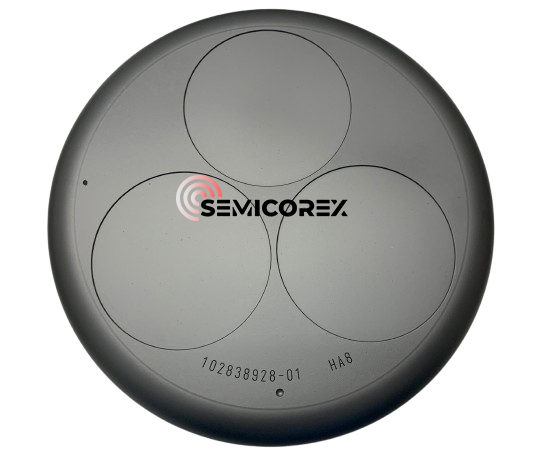
Every wafer that passes through a deposition chamber carries a hidden fingerprint of its thermal history. Slight gradients across the susceptor surface—often no more than a few degrees—can trigger uneven film growth, dopant drift, or residual stress that only becomes visible days later during probe testing. For years, these variations were tolerated as an unavoidable quirk of hardware. But as device geometries tightened, the margin for thermal sloppiness vanished. What used to be a background concern has pushed its way into the center of hardware engineering: how do you make a large, rotating plate hold a temperature so steady that the wafer never notices it is spinning?
The redesign efforts now underway are less about chasing a single perfect temperature and more about reshaping the thermal landscape itself. Engineers have moved beyond simply thickening the susceptor or swapping in a higher-purity graphite. They are carving out asymmetric pockets, embedding zone-controlled heating elements, and tuning edge compensation rings to counteract the natural heat loss at the rim. Some teams use transient thermal imaging to map hot spots during ramp-up, then feed that data into iterative coating thickness adjustments. The goal is not just an average temperature number that looks good on a spec sheet—it is a spatial uniformity that holds across the entire wafer, from center to edge, through every phase of the process.
The payoff shows up quietly in yield curves and final device reliability, not in dramatic press releases. A well-tuned susceptor can extend preventative maintenance intervals, reduce particle generation from thermal stress, and allow a process to run closer to its theoretical limit without crossing into defect territory. It is an innovation that operates in the background, invisible to anyone who does not look at the thermal maps, yet it often makes the difference between a process that merely works and one that works at scale with repeatable precision.
TaC and Beyond: Coating Breakthroughs That Keep Susceptors Alive Longer
The shift to tantalum carbide wasn't just a material upgrade—it rewrote the failure curve for graphite susceptors. In MOCVD and SiC epitaxy, repeated thermal cycling and exposure to hydrogen, silane, and ammonia slowly erode uncoated graphite, releasing particles that poison the wafer. A dense, crack-free TaC layer changes that equation. It resists the micro-fracturing that comes from thousands of ramp-up and cool-down cycles, and it does so without sacrificing the thermal uniformity that process engineers obsess over. The result is fewer particulate defects, longer intervals between maintenance, and a susceptor that can run hundreds of cycles past its graphite-only predecessor.
But the real story lies beyond binary “coated vs. uncoated” thinking. Newer work is pushing into layered and functionally graded coatings—where the top surface is TaC, but the underlying stack includes diffusion barriers or stress-relief interlayers to handle mismatch strain. Some teams are experimenting with ultra-thick TaC for aggressive chlorine-based cleaning, while others are modifying the carbide chemistry itself with small additions to alter grain growth during deposition. These aren’t cosmetic tweaks; they address the exact failure modes that still claim susceptors prematurely: edge delamination, thermal shock cracking, and localized pitting under high gas flow. By treating the coating not as a monolithic shell but as an engineered system, fabs are starting to see susceptor lifetimes that were unthinkable five years ago.
Shortening the Supply Chain: What China's Susceptor Makers Mean for Global Fabs
For years, the susceptor—a graphite or SiC-coated plate that holds wafers during epitaxial growth—has been quietly sourced from a handful of Japanese, German, and American suppliers. That's changing fast. Chinese manufacturers like SGL Carbon's local rivals and smaller domestic players are now shipping production-grade susceptors to domestic fabs, and increasingly to overseas customers. The immediate effect is a shorter physical supply chain: instead of waiting weeks for a susceptor to clear customs from Europe or Japan, a fab in Shanghai or Xi'an can receive replacements in days. But the shift goes beyond logistics. It's about control over a component that directly affects wafer uniformity and yield, and China's push to localize this piece of the equipment ecosystem is forcing global fabs to reconsider their own supplier maps.
The quality question remains the sticking point. Early Chinese susceptors struggled with coating delamination and inconsistent thermal conductivity, but that gap has narrowed substantially. Several Chinese makers now use isostatic pressing and CVD SiC coating lines that mirror processes used by established players, and some have passed qualification at leading-edge logic and memory fabs. What's different is the pace of iteration. Chinese suppliers tend to run shorter feedback loops with local fabs, tweaking graphite grades or coating thickness based on real production data. Global incumbents aren't standing still, but they rarely match that speed unless the customer is a top-tier fab. This dynamic is reshaping procurement strategies: even non-Chinese fabs are testing Chinese susceptors as a second source, not just for cost reasons but because having a supplier with spare capacity in Asia reduces the risk of a single-region bottleneck.
Strategically, the rise of China's susceptor makers signals a broader decoupling of subcomponent supply chains from traditional hubs. For a global fab, sourcing a Chinese susceptor isn't just a transactional decision; it means auditing a supplier that operates under different export control regimes and intellectual property norms. Yet ignoring them carries its own risk: if a major Chinese fab group standardizes on domestic susceptors, the volume and process data generated there could accelerate performance improvements that eventually make those parts attractive worldwide. The supply chain is shortening in more ways than one—geographically, yes, but also in terms of the time from process tweak to production deployment. For equipment engineers, that means closer collaboration with materials suppliers regardless of where they're located.
GaN, SiC, and Micro-LED: Versatile Susceptor Platforms for Emerging Epitaxy
Epitaxy rarely rewards a one-size-fits-all recipe. GaN, SiC, and micro-LED structures push growth reactors in different directions: GaN templates for micro-LED want ultra-smooth surfaces and low threading dislocation densities, SiC epilayers need precise control of polytype and doping uniformity, and GaN-on-SiC RF stacks must balance thermal expansion mismatch without cracking. When these material systems share a development line, they become a practical stress test for susceptor design, gas-phase chemistry, and temperature uniformity.
A closer look at thermal behavior explains why these platforms are so informative. SiC’s high thermal conductivity acts as a built-in heat spreader during high-temperature GaN growth, reducing wafer bow and enabling thicker buffer layers. Micro-LED’s tighter wavelength binning demands better in-situ reflectance and emissivity-corrected pyrometry across the entire susceptor surface. Meanwhile, GaN’s sensitivity to hydrogen and ammonia cracking forces reactor suppliers to rethink showerhead geometry and preheat zones. Each requirement feeds back into hardware that benefits all three.
Emerging epitaxy approaches—pulsed MOCVD, remote plasma-assisted growth, and selective area lateral overgrowth—are being evaluated first on these platforms because their defect signatures are well known. A subtle change in susceptor coating or ramp rate shows up quickly as a shift in yellow luminescence, carrier lifetime, or emission wavelength spread. That immediate, measurable feedback makes GaN, SiC, and micro-LED more than end products; they are diagnostic platforms for the next generation of epitaxial tools.
Integrated Flow and Heat: How Next-Gen MOCVD Susceptors Handle Extreme Workloads
Modern MOCVD reactors push susceptors to thermal and mechanical limits that older designs simply could not survive. The next generation of susceptors tackles this by embedding flow-directing microchannels directly into the graphite body, a move that turns passive heating into an active thermal management system. Instead of relying on uniform radiative heating alone, these channels route cooled purge gas through high-stress zones, shaving peak temperatures by tens of degrees while preserving the uniform wafer temperature profile that epitaxial growth demands. The result is a susceptor that handles repeated thermal cycling without warping or cracking, even when running at 1200°C and above for weeks on end.
What sets these designs apart is not just the cooling channels but how they interact with the reactor's gas flow. Traditional susceptors often suffer from recirculation zones near the edges, where precursor depletion and temperature drop combine to ruin thickness uniformity. Next-gen platforms use a combination of asymmetric pocket depths and micro-perforated rims to smooth the transition between the wafer and the exhaust path. The heat is extracted where the gas velocity is highest, naturally flattening the boundary layer. This integrated approach means a 6-inch GaN run can maintain a within-wafer temperature spread of under 2°C without external compensation heaters.
Field data from high-volume LED fabs shows the payoff: susceptor lifetime has doubled in many cases, while maintenance intervals stretch from weekly to monthly. One leading manufacturer reported a 40% drop in particle defects after switching to an integrated flow-and-heat design, attributed to reduced thermal stress spalling on the susceptor surface. The key is that the flow paths are laser-drilled and then sealed with a CVD SiC coating that matches the thermal expansion of the graphite core, preventing micro-cracks that used to plague earlier water-cooled attempts. For process engineers, that means fewer requalification runs and a recipe that stays stable across hundreds of growth cycles.
FAQ
The susceptor holds wafers during epitaxial growth and must maintain uniform temperature, resist aggressive gases, and avoid contamination. Any small flaw changes film thickness or doping, which directly affects device yield.
They are moving beyond simple graphite machining to advanced SiC coatings, better thermal design, and faster prototyping, which cuts lead times and costs for fabs that used to depend on a handful of foreign vendors.
There's growing use of high-purity graphite with denser SiC or TaC coatings, plus improved purification steps that reduce metal impurities. Some groups are also exploring composite designs to handle higher temperatures for GaN and SiC power devices.
The susceptor rotates and is heated by RF or resistance, but edge and center areas lose heat differently. Chinese manufacturers are using simulation-driven pocket shapes and variable coating thickness to narrow the temperature spread across the wafer.
GaN and SiC epi processes run at high temperatures and use corrosive precursors. Improved susceptor coatings reduce particle generation and extend service life, which keeps reactor uptime high and improves thickness uniformity for power electronics.
Some firms are adopting chemical vapor infiltration for coating, isostatic pressing for graphite blanks, and laser-based metrology for in-line pocket inspection. These reduce cracks and coating delamination compared to older methods.
Chinese equipment makers can now source susceptors locally, which shortens feedback loops between reactor design and consumable parts. That integration helps optimize pocket depth, wafer spacing, and gas flow as a single system.
Long-term reliability data and qualification at leading-edge nodes still favor established suppliers. Chinese makers need to prove that their coatings do not degrade after hundreds of thermal cycles and that impurity levels stay below strict limits.
Conclusion
China’s MOCVD susceptor suppliers are pushing single-crystal SiC beyond the lab and into production hardware. Monolithic structures remove the grain boundaries that plague polycrystalline graphite, giving fabs tighter control over thermal expansion and wafer-level temperature spread. That uniformity directly shapes defect counts and dopant consistency in GaN and SiC epi layers. On the coatings side, TaC remains the workhorse, but newer multilayer and mixed-carbide stacks are cutting metal contamination and extending service intervals enough to shift maintenance planning. Suppliers increasingly pair the susceptor with a tailored thermal model rather than selling a standalone part.
A parallel shift is happening in logistics. Domestic Chinese manufacturers now offer shorter lead times and on-site support that reduce a fab’s exposure to distant graphite specialists. Their susceptor platforms are also becoming more versatile, handling GaN-on-Si, SiC power, and Micro-LED processes that demand different balances of thermal mass and gas flow. Recent designs integrate flow channels and heat breaks directly into the susceptor body, keeping temperatures stable during long, high-power runs. The result is not just a replacement component but an architecture that evolves with next-generation MOCVD tools, reinforcing China’s broader role in compound semiconductor manufacturing.
Contact Us
Contact Person: Svenja Wei
Email: [email protected]
Tel/WhatsApp: +8613567891907
Website: https://www.semicorex.com